


Korean chipmaker investing US$4bn into US AI facility

08 April 2024
SK Hynix, a high-bandwidth memory (HBM) chipmaker based in South Korean, announced a US$3.87 billion investment for a plant in West Lafayette, Indiana, US, which will also serve as a research and development venue for Purdue University.
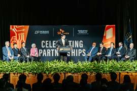 SK Hynix, on 3 April, announces semiconductor advanced packaging investment at Purdue Research Park. (Image: Purdue University/Kelsey Lefever)
The site will make advanced packaging fabrication for artificial intelligence (AI) products. It will house a semiconductor production line which will mass-produce dynamic random access memory (DRAM) chips, which the company said “are the critical components of graphic processing units that train AI systems such as ChatGPT.”
SK Hynix called the project the ‘first of its kind’ in the US, and said it expects the site to “drive innovation in the nation’s AI supply chain, while bringing more than a thousand new jobs to the region.”
Borrowing the term ‘Heartland’ (a nickname for the region of the US where Indiana is located), SK Hynix said it hopes to influence future tech development in the area.
“As this heterogeneous integration technology becomes more and more important to the future of the semiconductor industry, the company’s new initiative in Indiana will help establish the region as a Silicon Heartland: a new semiconductor cluster centred in the [US] Midwest… that will become a magnet for next-generation computing in the AI era.”
The company said production in the 430,000 sq ft (39,948m2) plant should start in the second half of 2028.
SK Hynix teams up with Purdue University
According to SK Hynix, the site was selected due to “Indiana’s resilient manufacturing infrastructure and R&D ecosystem, expert intellectuals in the semiconductor field and the talent pipeline at Purdue University, and the strong support provided by the state and local government.”
The company said several steps of collaboration with the university are already planned.
“These projects include work on advanced packaging and heterogeneous integration with Purdue’s Birck Nanotechnology Center and other research institutes and industry partners,” said SK Hynix. “They also hope to collaborate on a project related to memory-centric solutions and architecture for the generative AI era, specifically system-level memory design and in/near-memory computing.
SK Hynix added it will work with Purdue and Ivy Tech Community College (Indiana) to develop training programs and interdisciplinary degree curricula meant to cultivate a ‘high-tech workforce’ and build a pipeline for future talent.
Purdue University president Mung Chiang said, “This transformational investment reflects our state and university’s tremendous strength in semiconductors, hardware AI, and hard tech corridor. It is also a monumental moment for completing the supply chain of digital economy in our country through chips advanced packaging. Located at Purdue Research Park, the largest facility of its kind at a U.S. university will grow and succeed through innovation.”
STAY CONNECTED


Receive the information you need when you need it through our world-leading magazines, newsletters and daily briefings.
CONNECT WITH THE TEAM